
JNCASR Silicon Chip Carries Terahertz Data at 100 Gbit/s
JNCASR researchers built a silicon photonic crystal chip that pushes terahertz waves through an engineered barrier at 100 Gbit/s, pointing to 6G circuits.
Why in News
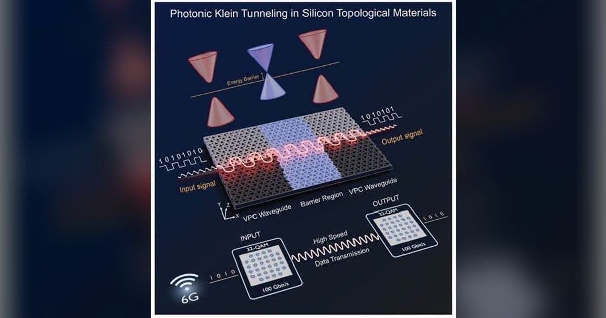
Researchers at JNCASR, Bengaluru, have shown a silicon photonic crystal chip on which terahertz waves pass through an engineered barrier with little loss while carrying data at 100 Gbit/s, a step towards compact circuits for future 6G networks.
Researchers at the Jawaharlal Nehru Centre for Advanced Scientific Research (JNCASR), an autonomous institute of the Department of Science and Technology, have demonstrated a silicon chip on which terahertz waves cross a deliberately built barrier with almost no loss while carrying data at 100 Gbit/s. The result points towards compact terahertz circuits for sixth-generation, or 6G, communication.
The problem being solved
Future 6G networks are expected to work at terahertz frequencies, which sit between microwaves and infrared light and offer very wide bandwidth. Routing such waves through small circuits is hard: bends, junctions and sudden changes in a waveguide scatter or reflect part of the signal and weaken it along the way.
What the team built
The group used topological photonics. Triangular holes were arranged in a silicon slab in a pattern that mimics the honeycomb lattice of graphene, creating a photonic crystal that guides terahertz waves along the boundary between two regions. A barrier was then formed simply by altering the sizes of the triangular holes over a short stretch of the waveguide, an effect known as photonic Klein tunnelling. One such barrier added only about one to two per cent loss, and two barriers in sequence about two to three per cent, where an ordinary non-topological waveguide would have cut transmission sharply. Transmission stayed near its barrier-free level so long as the barrier strength remained below a characteristic coupling strength of the crystal, which gives designers a usable rule of thumb.
The devices and the speeds
Three devices were fabricated on high-resistivity silicon, a material that suits established semiconductor manufacturing: one with two barriers in sequence, one with an omega-shaped route holding four sharp bends and a central barrier, and a power splitter with a barrier in one branch. Measurements over 310 to 360 GHz matched simulations closely. The double-barrier device carried 48 Gbit/s and the omega-shaped one 60 Gbit/s, while the splitter reached 100 Gbit/s using QAM-32 modulation, a rate at which a five-gigabyte film could in principle move in under half a second.
Who did the work
The study was led by Dr Abhishek Kumar of JNCASR, who heads the Meta Optics Laboratory, with Samina Mulla and Sangram Kumar Sadhu as joint first authors. Collaborators came from IISER Kolkata, IIT Bombay, the Institute of Microelectronics at A*STAR in Singapore and the University of Lille with CNRS in France. The work appeared in the journal Advanced Materials.
Important Facts
| Institute | Jawaharlal Nehru Centre for Advanced Scientific Research (JNCASR) |
|---|---|
| Parent department | Department of Science and Technology (DST) |
| Achievement | Terahertz data transmission at 100 Gbit/s across an engineered barrier |
| Technology | Topological photonics; photonic Klein tunnelling in a silicon photonic crystal |
| Frequency range tested | 310 to 360 GHz |
| Device speeds | Double-barrier 48 Gbit/s, omega-shaped 60 Gbit/s, splitter 100 Gbit/s |
| Lead researcher | Dr Abhishek Kumar, Meta Optics Laboratory, JNCASR |
| Journal | Advanced Materials |
| Application | Compact terahertz circuits for future 6G communication |
Exam Point of View
Remember the institute (JNCASR, under the Department of Science and Technology), the technology (topological photonics and photonic Klein tunnelling in a silicon photonic crystal), the data rate of 100 Gbit/s, the measured band of 310 to 360 GHz, the use of terahertz frequencies in 6G, the graphene-like honeycomb lattice design, the lead researcher Dr Abhishek Kumar and the journal Advanced Materials.
Practice Questions
Which institute developed the silicon chip that carried terahertz data at 100 Gbit/s across an engineered barrier?
- A.Indian Institute of Science, Bengaluru
- B.Jawaharlal Nehru Centre for Advanced Scientific Research
- C.Saha Institute of Nuclear Physics, Kolkata
- D.Centre for Development of Telematics
Show answer
Its team, led by Dr Abhishek Kumar of the Meta Optics Laboratory, used topological photonics to show terahertz waves crossing a deliberately engineered barrier while carrying data at 100 Gbit/s, with the work published in the journal Advanced Materials.
Read the full explanation →The silicon photonic crystal used in the JNCASR work was patterned to mimic the lattice of which material?
- A.Diamond
- B.Graphene
- C.Gallium nitride
- D.Sapphire
Show answer
The team designed a silicon photonic crystal whose structure mimics the honeycomb lattice of graphene, arranging triangular holes in a silicon slab so that terahertz waves travel along the boundary between two regions of the crystal.
Read the full explanation →Over which frequency range were the JNCASR terahertz devices measured?
- A.24 to 40 GHz
- B.110 to 170 GHz
- C.310 to 360 GHz
- D.600 to 750 GHz
Show answer
Measurements across this band agreed closely with the simulations the team had run, and in the power splitter the two output signals were nearly identical, showing that the engineered barrier had little effect on transmission.
Read the full explanation →Frequently Asked Questions
What did JNCASR researchers demonstrate on their silicon chip?
That terahertz waves can cross an engineered barrier with very little loss while carrying data at 100 Gbit/s, which supports the design of compact terahertz circuits for 6G networks.
Why are terahertz frequencies important for 6G?
They lie between microwaves and infrared light and offer very wide bandwidth. The difficulty is guiding them through small circuits, because bends and junctions scatter or reflect the signal.
How was the barrier created on the chip?
By changing the sizes of the triangular holes over a short section of the waveguide in a silicon photonic crystal whose structure mimics the honeycomb lattice of graphene.
Sources
- https://www.pib.gov.in/PressReleasePage.aspx?PRID=2332613 (opens in a new tab) — Press Information Bureau
Current Affairs 4 November 2026
- India-Poland Trade Push: Jitin Prasada Visits WarsawInternational
- NLMC Phase II RINL Land Auction Fetches Rs 218 CroreEconomy
- Railways Freight Loading Hits 145.07 MT in October 2026Economy
- CSIR and DAKSHIN-RIS Sign Pact for Global South ScienceScience & Technology
- Ayush Minister Ties Dhanteras to Preventive HealthcareImportant Days
- Schedule M Amendment Aligns Grade A Limits With WHO NormsNational
- Cabinet Clears Rs 2,814 Crore Critical Mineral Capex SchemeGovernment Schemes
- Cabinet Approves Rs 4,371.10 Crore VISTAR Statistics SchemeEconomy
Related Current Affairs
- Science & Technology
India Plans First Human Deep-Sea Mission to 6,000 m by 2028
4 November 2026 · 2 min read
- Science & Technology
TRAI Launches Network Anubhav Platform for Network Quality
4 November 2026 · 2 min read
- Science & Technology
CSIR and DAKSHIN-RIS Sign Pact for Global South Science
4 November 2026 · 2 min read
- Science & Technology
IndiaAI Mission Releases EKA-1 and Dhir Foundation Models
3 November 2026 · 2 min read
- Science & Technology
Aditya-L1 VELC Finds Solar Eruption Expands Asymmetrically
3 November 2026 · 2 min read




Related GK
- Famous Personalities of Rajasthan: Exam Notes
28 October 2026 · Rajasthan
- Districts and Divisions of Rajasthan: Exam Notes
28 October 2026 · Rajasthan
- Tourism and World Heritage Sites of Rajasthan Notes
27 October 2026 · Rajasthan
Take the Quiz
- Current Affairs Quiz
Defence Current Affairs Quiz: 4 November 2026
12 questions12 minutesStart Quiz